Potting & Encapsulation
Potting & Encapsulation for optimal reliability
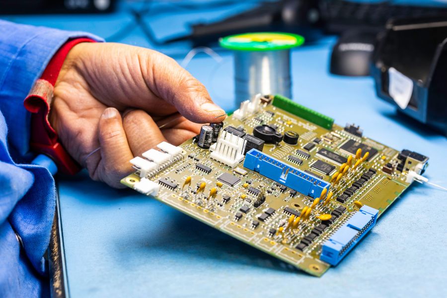
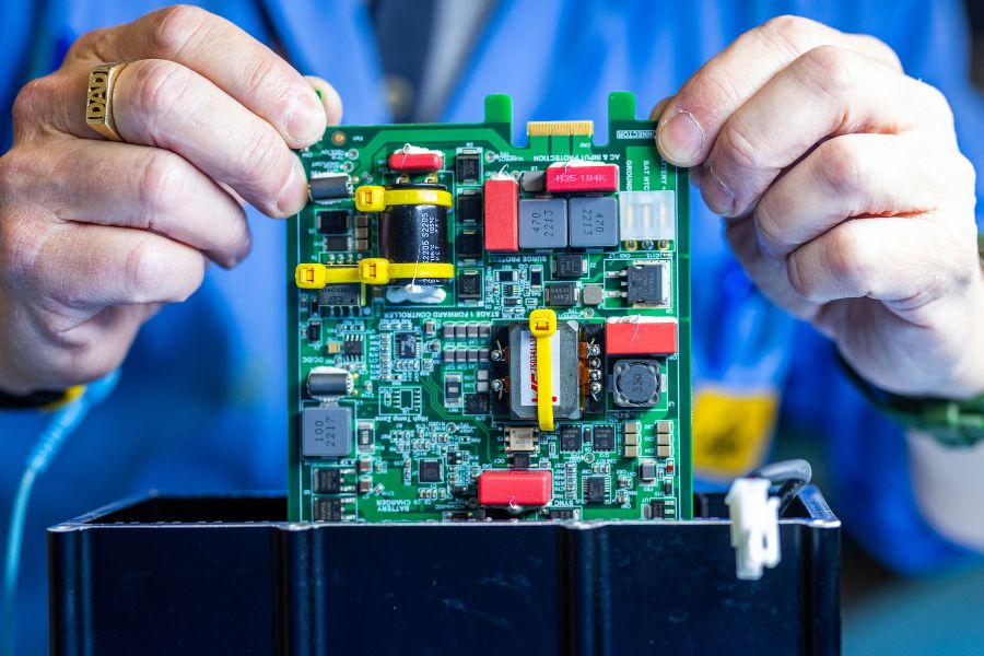
The potting and encapsulation of printed circuit board assemblies are indispensable elements of your electronic product’s manufacturing process, crucially influencing product reliability.
Protecting your PCB assembly
Electronics potting is the process of immersing the completed electronic assembly within a protective solid or gelatinous material. Depending on the application of your PCBA, there are three commonly used materials available – epoxy, polyurethane and silicone.
During the electronics potting process, an assembly is diligently placed within a mould, referred to as the ‘pot’. This mould serves as a container and shaping tool throughout the potting process. The pot is filled with the selected potting material or compound which, once cured or hardened, permanently encapsulates and shields the electronic assembly.
Contact our specialist team to discuss your PCB assembly & Box Build requirements
Although the terms electronics ‘potting’ and ‘encapsulation’ are often used interchangeably, their end result varies. Potting refers to a process whereby the pot that is filled with the compound becomes a part of the finished board. In encapsulation, the component and hardened resin are removed from the pot to be placed into an assembly.
Expert advice to guide your design
The choice of PCBA protective system is vital to the design and development of your electronic product. Which one you need depends on a number of manufacturing and application factors, and MPE’s experienced team is readily available to advise you.

PCB Assembly
Precise, reliable PCB assembly to your exact requirements.

Box Build Assembly
Optimise your supply chain with our turnkey assembly service.
